


The semiconductor manufacturing process is arguably the most precision-dependent industrial environment on earth. As wafer nodes shrink to sub-5 nanometers, the tolerance for particulate contamination, ionic leaching, and fluid flow instability drops to absolute zero. Within the cleanroom environment, the transportation of ultrapure water (UPW), aggressive chemical etchants, and chemical mechanical planarization (CMP) slurries requires specialized fluid delivery architecture.
Standard industrial fluid equipment cannot meet these stringent baseline requirements. Micro-vibrations, trace metal leaching from pump casings, or microscopic seal wear can instantly destroy millions of dollars of wafer inventory. To maintain acceptable yield rates, fabrication plants (fabs) must deploy dedicated semiconductor pump solutions engineered explicitly for extreme purity and absolute containment. This technical overview breaks down the critical requirements, material science, and mechanical configurations necessary for specifying fluid transfer systems in the microelectronics industry.

1. The Critical Need for Advanced Semiconductor Pump Solutions
In a modern fab, liquids are constantly in motion. From the bulk chemical delivery systems (BCDS) located in the sub-fab to the precise point-of-use dosing on the process tools, the integrity of the fluid must be perfectly maintained. An advanced semiconductor pump solution is not merely a transfer mechanism; it is an active contamination-prevention boundary.
The primary engineering challenge is moving highly corrosive media—such as hydrofluoric acid (HF), sulfuric acid, and hydrogen peroxide—without introducing metallic ions or shedding polymer particulates into the fluid stream. This requires a fundamental departure from conventional mechanical seal pumps. Furthermore, as production throughput increases, these systems must operate continuously for 24/7 duty cycles with a predictable, ultra-low maintenance profile to avoid taking critical process tools offline.

2. Overcoming Contamination with High-Purity Pumping Systems
Contamination in microelectronics fluid transfer primarily originates from two sources: mechanical wear and chemical leaching. Traditional mechanically sealed pumps rely on the physical contact of carbon or ceramic faces, which inevitably shed microscopic particles into the fluid during operation.
High-purity pumping systems eliminate this risk by adopting completely sealless architectures. Furthermore, the wetted components of the pump must be manufactured from virgin, unfilled polymers. Any additives, UV stabilizers, or carbon fillers commonly used in standard industrial plastics will leach into ultrapure water or aggressive solvents. By utilizing specific molding techniques in cleanroom environments, pump manufacturers ensure that the internal surfaces are microscopically smooth, eliminating micro-crevices where bacteria or chemical residues could accumulate and subsequently contaminate the process loop.

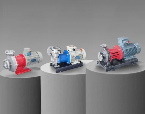
3. Sealless Mag-Drive Pumps for Microelectronics Fluid Transfer
The industry standard for handling hazardous and ultrapure fab chemicals is the magnetic drive configuration. Sealless mag-drive pumps for microelectronics fluid transfer replace the dynamic mechanical shaft seal with a static, non-permeable containment shell.
In this configuration, a synchronous magnetic field transmits the motor's torque across the containment barrier to the internal impeller. Because there is no rotating shaft penetrating the casing, the leak path to the atmosphere is entirely removed. This absolute containment is critical not only for protecting the purity of the internal fluid but also for protecting cleanroom personnel and sensitive adjacent electronics from exposure to toxic chemical fumes. The internal bearings, lubricated solely by the process fluid, are typically constructed from high-purity silicon carbide to prevent particulate generation.

4. Material Selection in Wafer Fabrication Liquid Delivery Solutions
The chemical compatibility and ionic stability of the pump's wetted path dictate its suitability for semiconductor applications. Wafer fabrication liquid delivery solutions rely heavily on advanced fluoropolymers.
For extreme chemical resistance and high-purity requirements, Perfluoroalkoxy (PFA) and Polytetrafluoroethylene (PTFE) are the materials of choice. Unlike standard plastics, these fluoropolymers exhibit near-universal chemical inertness and have exceptionally low trace-metal extractables.
| Process Fluid Category | Typical Fab Chemicals | Required Pump Metallurgy / Polymer |
| Ultrapure Water (UPW) | 18.2 MΩ-cm DI Water | Virgin PFA, PTFE, or PVDF |
| Acidic Etchants | Hydrofluoric Acid, Sulfuric Acid | High-purity PFA lined, Silicon Carbide internals |
| Solvents | Isopropyl Alcohol (IPA), Acetone | PTFE lined or 316L Stainless Steel (depending on grade) |
| CMP Slurries | Silica or Alumina based abrasive slurries | specialized Polyurethane or low-shear PD structures |
5. Managing Thermal Control in Semiconductor Fab Pumping Equipment
Many wafer fabrication processes, particularly etching and deposition, require highly precise temperature regulation. Chillers and heat exchangers are deployed to circulate thermal fluids (such as specialized fluorinated liquids or water/glycol mixtures) to the process chamber chucks.
Semiconductor fab pumping equipment used in these thermal control loops faces significant thermal cycling. The pumps must maintain structural stability and alignment across rapid temperature shifts without warping or causing bearing stress. Furthermore, the pumps must not impart excess heat into the thermal fluid. If a magnetic drive pump utilizes a metallic containment shell, the rotating magnetic field generates eddy currents, which introduce unwanted heat into the fluid. To maintain strict temperature control, high-end semiconductor pumps utilize non-metallic containment shells (such as carbon-fiber reinforced plastics) that eliminate eddy current heat generation entirely.

6. Handling Aggressive Etchants with Chemical Processing Pump Solutions
The wet bench is the heart of the wafer cleaning and etching process. Here, highly concentrated, heated acids are circulated over the wafer surface to remove oxides and photoresist. Handling these aggressive etchants with chemical processing pump solutions requires extreme structural safety factors.
If a pump casing were to rupture while circulating 80°C sulfuric acid, the result would be catastrophic. To prevent this, semiconductor-grade pumps often utilize a dual-containment design. The inner wetted layer is composed of thick, injection-molded PFA for chemical resistance, while the outer structural armor is cast from ductile iron. This hybrid construction ensures that the pump can withstand high system pressures and mechanical piping strain while completely isolating the metal from the corrosive process media.

7. Flow Stability and Pulsation Control in Chip Manufacturing Pumps
Certain semiconductor processes, particularly spin coating and photolithography, require absolute flow stability. Any pulsation or pressure spiking in the fluid delivery line will cause uneven coating thickness on the wafer, destroying the batch.
To achieve maximum flow stability in chip manufacturing pumps, centrifugal technologies are often heavily favored over standard volumetric pumps, as they naturally provide a smooth, continuous flow curve. When variable flow rates are required, these pumps are paired with precision Variable Frequency Drives (VFDs). The pump's impeller geometry must be optimized using computational fluid dynamics (CFD) to ensure the hydraulic transition from the suction eye to the discharge volute is completely laminar, preventing micro-cavitation and flow ripple.

8. Customizing Cleanroom Fluid Handling Solutions for Your Facility
Because space within the sub-fab is sold at an extreme premium, pumping equipment must often conform to strict dimensional footprints and specific piping orientations. Customizing cleanroom fluid handling solutions requires a manufacturer capable of rapid engineering adaptation.
This includes adjusting flange orientations, integrating specific leak-detection sensors into the pump casing, and modifying the motor adapter to accept specialized cleanroom-rated motors. When evaluating infrastructure upgrades, adhering to the safety and design standards published by Semiconductor Equipment and Materials International is an absolute necessity. By partnering with a pump manufacturer that understands the unique constraints of the microelectronics industry, fab operators can secure the fluid reliability necessary for next-generation wafer production.